
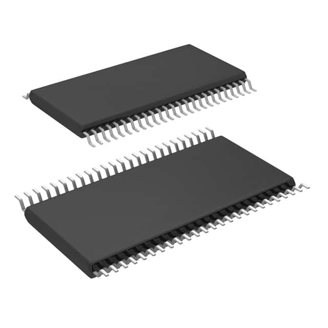
The CLVC16T245MDGGEP is a high-performance 16-bit noninverting bus transceiver engineered for universal low-voltage bidirectional voltage translation, categorized as an enhanced-product logic IC within Texas Instruments' SN74LVC16T245-EP series[reference:0][reference:1]. Packaged in a compact 48-pin TSSOP (DGG) surface-mount housing optimized for automated SMT assembly[reference:2][reference:3], this device is capable of building scalable multi-voltage communication bridges by coordinating with two independent configurable power-supply rails, supporting seamless data translation between 1.8‑V, 2.5‑V, 3.3‑V, and 5‑V logic nodes[reference:4][reference:5].
Its core advantage lies in the fully configurable dual-rail design, which allows each port to operate independently across the full 1.65‑V to 5.5‑V supply range[reference:6]. Unlike most single-supply level shifters, this device integrates two separate power-supply rails (VCCA for the A port and VCCB for the B port)[reference:7], enabling flexible construction of bidirectional translation pathways between any combination of low-voltage nodes without requiring complex external biasing networks. This significantly shortens hardware development cycles for multi-voltage system interfaces, from microcontroller peripherals to memory modules and communication buses[reference:8].
Embedded within the chip is a direction‑control and output‑enable logic architecture referenced to VCCA. Engineers can configure data flow direction via the DIR input and place outputs into high‑impedance mode via the OE input, effectively implementing bidirectional data flow with common control for two 8‑bit ports[reference:9][reference:10]. The device transmits data from the A bus to the B bus when the B‑port outputs are activated, and from the B bus to the A bus when the A‑port outputs are activated[reference:11]. The input circuitry on both ports always remains active, requiring a valid logic HIGH or LOW level to prevent excess supply current[reference:12].
The device is equipped with comprehensive power‑down and isolation protection mechanisms as standard configurations. The Ioff circuitry disables the outputs when the device is powered down, preventing damaging current backflow through the device[reference:13][reference:14]. Additionally, the VCC isolation feature ensures that if either VCC input is at GND, both ports are placed into the high‑impedance state, effectively isolating the bus and protecting the entire system from unintended signal contention or parasitic conduction[reference:15][reference:16]. To guarantee the high‑impedance state during power‑up or power‑down, the OE pin should be tied to VCC through a pull‑up resistor[reference:17].
The device accepts a wide input supply range from 1.65 V up to 5.5 V on both VCCA and VCCB rails, adapting to various low‑voltage DC power domains in mixed‑voltage systems[reference:18][reference:19]. Its operating temperature range covers ‑55 °C to 125 °C, ensuring stable performance under extreme ambient conditions for military‑grade and industrial equipment[reference:20][reference:21]. The device supports a maximum output current of ±32 mA per channel with a propagation delay of 27.8 ns (typical)[reference:22][reference:23][reference:24], and features overvoltage‑tolerant inputs and outputs that allow mixed‑voltage‑mode data communications[reference:25]. ESD protection exceeds JESD 22 specifications, including 2000‑V Human‑Body Model and 1000‑V Charged‑Device Model[reference:26]. The component complies with RoHS and REACH environmental directives, adopts a NiPdAu lead‑free metallization finish[reference:27], and has passed Moisture Sensitivity Level‑1 certification (MSL‑1), supporting unlimited reflow soldering production standards[reference:28][reference:29].
Common application scenarios include industrial communication networks, automotive systems, building automation, data communication interfaces, memory modules, medical instrumentation, and consumer electronics[reference:30][reference:31][reference:32]. Typical use cases involve bridging a 5‑V UART transceiver to a 3.3‑V host microcontroller, level‑shifting GPIO signals between FPGA and peripheral sensors, and interfacing memory modules with processors operating at different I/O voltages[reference:33][reference:34]. Thanks to its flexible dual‑rail topology, comprehensive power‑down protection, and reliable wide‑temperature stability, the CLVC16T245MDGGEP has become a mainstream choice for high‑speed, high‑reliability voltage‑translation and bus‑interface design schemes in mission‑critical systems[reference:35].