
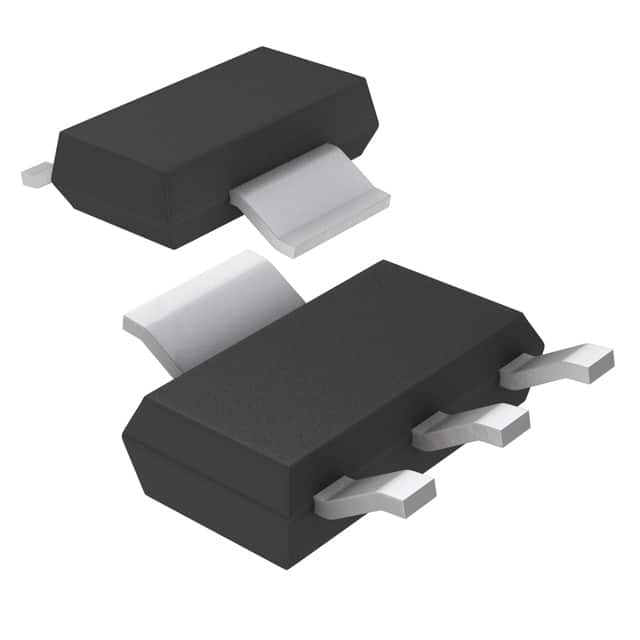
Designed as a cost‑effective 5V linear regulator solution, the LT1123CST#PBF is a 3‑pin bipolar driver IC engineered to work in conjunction with an external PNP power transistor, forming an inexpensive, high‑current Low Dropout linear regulator[reference:0]. Categorized as a versatile regulator driver within Analog Devices' (formerly Linear Technology) power management portfolio, this device is available in a compact 3‑pin SOT‑223 surface‑mount package (ST suffix) as well as a low‑cost TO‑92 package (CZ suffix), offering flexibility for both automated SMT assembly and through‑hole prototyping[reference:1][reference:2]. By pairing with a suitable external PNP pass transistor, the LT1123 can deliver guaranteed output current up to 4A, making it an ideal choice for powering noise‑sensitive loads where switching regulators are impractical[reference:3].
The core advantage of this Low Dropout regulator driver lies in its extremely low dropout voltage performance[reference:4]. When configured with an external PNP pass transistor such as the MJE1123, the dropout voltage is as low as 0.3V at 1A output current, and only 0.5V at the full 4A load[reference:5]. This ultra‑low headroom requirement greatly reduces power dissipation caused by voltage conversion loss, improving overall system energy efficiency-particularly in battery‑powered or low‑voltage industrial applications. Unlike many integrated linear regulators that force designers to accept fixed pass‑transistor limitations, the LT1123's external‑transistor topology allows engineers to tailor the pass element to their specific current and thermal requirements, significantly enhancing design flexibility.
At the heart of the LT1123 is a trimmed bandgap reference and an error amplifier, delivering a fixed 5V output trimmed to ±1% accuracy at room temperature, with a guaranteed tolerance of ±2% over the full operating temperature range[reference:6][reference:7][reference:8]. The internal driver circuit is capable of sinking up to 125mA from the base of the external PNP pass transistor[reference:9]. A unique feature of this driver is its drive‑current foldback mechanism: as the feedback pin approaches ground, the available drive current is reduced, effectively limiting the base drive under short‑circuit conditions and protecting the pass transistor from excessive stress[reference:10]. The drive pin also serves as the supply input for the device's internal circuitry, including start‑up, bias, current limit, and thermal limit functions, with a typical minimum drive current of only 450µA[reference:11].
The LT1123 is equipped with comprehensive protection mechanisms as standard features. An internal thermal limit circuit safeguards the device against excessive power dissipation, while the built‑in current limiting-enhanced by the foldback characteristic-prevents damage during output overload or short‑circuit events[reference:12][reference:13]. The device's robust design is further reflected in its absolute maximum ratings: the drive pin and feedback pin can both withstand up to 30V, and the storage temperature ranges from –65°C to 150°C[reference:14]. The operating junction temperature spans 0°C to 125°C, ensuring reliable performance across a wide range of ambient conditions[reference:15].
The LT1123 accepts a wide input voltage range, with the drive pin capable of handling up to 30V[reference:16]. It draws a remarkably low quiescent current of only 700µA, making it well‑suited for always‑on or battery‑backed applications where standby power consumption is a critical concern[reference:17][reference:18]. Key electrical specifications include 1mV line regulation and 5mV load regulation, ensuring a stable 5V output even under varying input and load conditions[reference:19][reference:20]. The device's output voltage temperature coefficient is a mere 0.2mV/°C, contributing to excellent thermal stability[reference:21]. The SOT‑223 package offers a thermal resistance of approximately 20°C/W when the tab is properly soldered to the PCB, enabling efficient heat dissipation[reference:22]. The component complies with RoHS environmental directives and is available in a lead‑free finish (denoted by the #PBF suffix).
Common application scenarios for this 5V linear regulator driver include industrial embedded power modules, automotive electronics, portable instrumentation, sealed lead‑acid battery chargers, and post‑regulation for switching power supplies where low output noise is paramount[reference:23]. Typical use cases involve building a 5V/4A regulator with an MJE1123 pass transistor and a few external components-a resistor (RD) to reduce base drive and minimize power dissipation in the LT1123, along with input and output capacitors for stability[reference:24][reference:25]. The flexible external‑transistor topology also allows designers to select pass transistors with different current ratings or package types to optimise for cost, thermal performance, or board space. Thanks to its Low Dropout architecture, low quiescent current, ±1% output accuracy, and robust protection features, the LT1123CST#PBF has become a trusted choice for engineers seeking a simple, reliable, and cost‑effective 5V linear regulator solution-one that delivers linear‑regulator cleanliness with the current capability usually reserved for switching converters, all while maintaining the simplicity of a 3‑pin driver IC.