Professional testing equipment and reports to ensure product quality.
Analog Devices Inc. RFQ AVAILABLE

LT8365JMSE#TRPBF

IC REG BST SEPIC TRAN DRV 16MSOP

Part Number
LT8365JMSE#TRPBF
Manufacturer
Analog Devices Inc.
Category
Voltage Regulators - DC DC Switching Regulators
Package
16-TFSOP (0.118", 3.00mm Width), 12 Leads, Exposed Pad
Datasheet:
LT8365JMSE#TRPBF.pdf
Description
IC REG BST SEPIC TRAN DRV 16MSOP
Select Quantity Stock: 12,168

FAST RESPONSE

Quick RFQ

Send your requirements and our sales team will contact you as soon as possible.

Part Number
Quantity *
Target Price
Name *
Company *
Email *
Comments
PRODUCT INFORMATION

Product Details

PRODUCT TECHNICAL REFERENCE

LT8365JMSE#TRPBF Low IQ Boost/SEPIC/Inverting Converter with 1.5A, 150V Switch

A comprehensive technical overview of the LT8365JMSE#TRPBF, a current mode DC/DC converter from Analog Devices featuring an integrated 1.5A, 150V switch, a wide 2.8V to 60V input voltage range, an ultralow 9µA quiescent current in Burst Mode® operation, a unique single feedback pin architecture for positive or negative output programming, programmable frequency from 100kHz to 500kHz, spread spectrum frequency modulation (SSFM) for low EMI, and a thermally enhanced 16-lead MSOP package. The J-grade version is specified for operation from –40°C to +150°C junction temperature. Covers device function, core features, electrical specifications, pin configuration, typical applications, and replacement selection guidance.

Analog Devices 16(12)-Lead MSOP-EP (3mm × 3mm) 2.8V to 60V
Device Classification Boost/SEPIC/Inverting DC/DC Converter
Part Number
LT8365JMSE#TRPBF
Mounting Type
Surface Mount
Operating Temperature Range
-40°C to +150°C (TJ)
01
PRODUCT OVERVIEW

What Is the LT8365JMSE#TRPBF?

LT8365JMSE#TRPBF is a current mode DC/DC converter from Analog Devices with an integrated 1.5A, 150V power switch, designed to operate from an input voltage range of 2.8V to 60V. The device features a unique single feedback pin (FBX) architecture that enables easy configuration as a boost, SEPIC, or inverting converter with either positive or negative output voltage programming.

In Burst Mode® operation, the LT8365 consumes as little as 9µA of quiescent current at very low output currents while maintaining high efficiency, with typical output ripple below 15mV. The switching frequency is programmable from 100kHz to 500kHz via a single resistor on the RT pin, and the SYNC/MODE pin allows synchronization to an external clock as well as selection between pulse-skipping and Burst Mode operation, with or without spread spectrum frequency modulation (SSFM) for low EMI.

Additional features include a BIAS pin that accepts a second input supply to power the INTVCC regulator for improved efficiency, frequency foldback, and programmable soft-start to control inductor current during start-up. The device is AEC-Q100 qualified for automotive applications.

The LT8365JMSE#TRPBF is the J-grade version in a thermally enhanced 16-lead MSOP package with four pins removed (12 active leads plus an exposed pad) to provide high-voltage pin spacing. It is specified for operation from –40°C to +150°C junction temperature. The device is RoHS compliant, REACH unaffected, and in active production.

Wide 2.8V to 60V Input Range Integrated 1.5A, 150V switch supports boost, SEPIC, and inverting topologies with a unique single feedback pin for positive or negative output programming.
Ultralow Quiescent Current (9µA) Burst Mode® operation draws only 9µA at no load while maintaining output ripple below 15mV, ideal for always-on and battery-powered systems.
Low EMI & Programmable Frequency Programmable 100kHz to 500kHz frequency with SSFM for low EMI, external synchronization, and a BIAS pin for improved efficiency. AEC-Q100 qualified.
02
DEVICE HIGHLIGHTS

Key Features and Benefits of LT8365JMSE#TRPBF

Wide 2.8V to 60V Input Range

Operates from 2.8V to 60V input, supporting a broad spectrum of applications including automotive, industrial, telecom, and portable electronics.

Integrated 1.5A, 150V Switch

The integrated high-voltage power switch simplifies the design of boost, SEPIC, and inverting converters, eliminating the need for external switching components.

Ultralow Quiescent Current (9µA)

Burst Mode® operation draws only 9µA of quiescent current at very low output currents while keeping output ripple below 15mV, extending battery life in always-on systems.

Single Feedback Pin (FBX) Architecture

The unique FBX pin enables easy programming of either positive or negative output voltages, simplifying the configuration of boost, SEPIC, and inverting topologies.

Programmable Frequency & SSFM

Switching frequency is programmable from 100kHz to 500kHz, with spread spectrum frequency modulation (SSFM) available for low EMI, and synchronization to an external clock via the SYNC/MODE pin.

AEC-Q100 Qualified & J-Grade

AEC-Q100 qualified for automotive applications with the J-grade specified for –40°C to +150°C junction temperature, housed in a thermally enhanced 16-lead MSOP package with high-voltage pin spacing.

03
REFERENCE DATA

Technical Specifications for LT8365JMSE#TRPBF

Part Number LT8365JMSE#TRPBF Manufacturer Analog Devices
Device Type Boost/SEPIC/Inverting DC/DC Converter Topology Boost, SEPIC, Inverting
Input Voltage Range (VIN) 2.8V to 60V Maximum Switch Voltage 150V
Switch Current (Max) 1.5A Output Voltage Configuration Positive or Negative (via FBX)
Quiescent Current (IQ) 9µA (Burst Mode®) Output Ripple (Burst Mode®) < 15mV (Typical)
Switching Frequency Range 100kHz to 500kHz External Synchronization Yes (via SYNC/MODE)
Spread Spectrum SSFM (for Low EMI) Feedback Voltage (FBX) 1.60V (Internal Bias)
BIAS Pin Second Input for INTVCC (Improves Efficiency) Soft-Start Programmable (External Capacitor)
EN/UVLO Pin Shutdown and Programmable UVLO INTVCC Regulator 3.8V Internal Supply
Package / Case 16(12)-Lead MSOP with Exposed Pad Supplier Device Package MSOP-EP (MSE16-12)
Pin Count 12 Active Leads + Exposed Pad Mounting Type Surface Mount
Operating Junction Temperature (J-Grade) -40°C to +150°C AEC-Q100 Qualification Yes
RoHS ROHS3 Compliant REACH Status REACH Unaffected
MSL Level MSL 1 (Unlimited) Product Status Active
Packaging Tape & Reel (2,500 per Reel) Grade J-Grade

Electrical values shown above are reference values. Test conditions, limits, and guaranteed performance should always be confirmed from the current official manufacturer datasheet before design or production use.

04
DESIGN REFERENCE

Circuit Considerations for LT8365JMSE#TRPBF

Topology, Frequency & Mode Configuration

The LT8365JMSE#TRPBF offers flexible configuration for topology, frequency, and operating mode:

  • Topology Selection (FBX Pin): The single FBX feedback pin supports positive or negative output programming, enabling boost, SEPIC, or inverting configurations with minimal external components.
  • Switching Frequency (RT Pin): A resistor from RT to the exposed pad GND (near FBX) programs the switching frequency from 100kHz to 500kHz.
  • Mode & Synchronization (SYNC/MODE Pin): Selects between Burst Mode, pulse-skipping, or SSFM operation. Tie to GND for Burst Mode, apply an external clock for synchronization, use a 100kΩ resistor for Burst/SSFM, float for pulse-skipping, or tie to INTVCC/>1.7V for pulse-skipping/SSFM.
  • Soft-Start (SS Pin): A capacitor from SS to GND (near FBX) controls the ramp rate of inductor current during start-up (charging current is 2µA).
  • Enable/UVLO (EN/UVLO Pin): A resistor divider from VIN programs the undervoltage lockout threshold. Below the accurate 1.6V threshold, the part enters UVLO; below 0.2V, VIN current drops below 1µA.

PCB and System-Level Guidance

High-voltage converter performance depends on layout and component selection:

  • Input Capacitor: Locally bypass the VIN pin with a low-ESR ceramic capacitor placed as close as possible to the pin and the exposed pad PGND copper.
  • INTVCC Capacitor: Bypass the INTVCC pin with a 1µF low-ESR ceramic capacitor to GND. No additional components or loading are allowed on this pin.
  • BIAS Pin: Connect a second input supply (4.4V ≤ BIAS ≤ 60V) to improve efficiency by powering the INTVCC regulator from BIAS instead of VIN.
  • Exposed Pad: The exposed pad is the power ground (PGND) and signal ground (GND). It must be soldered to the PCB ground plane for thermal and electrical performance.
  • High-Voltage Spacing: The package removes four pins to provide high-voltage pin spacing. Maintain appropriate creepage and clearance distances on the PCB for the 150V switch node.
  • Verify the recommended PCB footprint from the official datasheet prior to production.
05
16(12)-LEAD MSOP-EP (3mm × 3mm)

Pin Configuration Reference for LT8365JMSE#TRPBF

LT8365
MSOP TOP VIEW

Confirm package orientation and pin numbering against the official package drawing before PCB layout. The MSE16 package has 16 lead positions with four pins removed (12 active leads) plus an exposed pad (Pin 17) to provide high-voltage pin spacing. The exposed pad must be soldered to the PCB ground plane for thermal and electrical performance.

1 VIN Input Supply - Must Be Locally Bypassed with Low-ESR Ceramic Capacitor
2 EN/UVLO Shutdown and Undervoltage Detect - Below 1.6V Enters UVLO; Below 0.2V Reduces VIN Current Below 1µA
3 SS Soft-Start - Capacitor to GND (Near FBX) Controls Inductor Current Ramp Rate; 2µA Charging Current
4 RT Oscillator Frequency Program - Resistor to Exposed Pad GND (Near FBX) Sets 100kHz to 500kHz
5 SYNC/MODE Mode Selection and Synchronization - Selects Burst, Pulse-Skipping, or SSFM; Accepts External Clock
6 BIAS Second Input Supply for INTVCC - Connect to 4.4V–60V Rail for Improved Efficiency
7 INTVCC Regulated 3.8V Internal Supply - Bypass with 1µF Low-ESR Ceramic Capacitor to GND
8 FBX Voltage Regulation Feedback - Single Pin for Positive or Negative Output Programming
9 NC No Connect - Pin Removed for High-Voltage Spacing
10 NC No Connect - Pin Removed for High-Voltage Spacing
11 SW2 Switch Node - Internal Power Switch Connection (Paired with SW1)
12 SW1 Switch Node - Internal Power Switch Connection (Paired with SW2)
13 NC No Connect - Pin Removed for High-Voltage Spacing
14 NC No Connect - Pin Removed for High-Voltage Spacing
15 GND Signal Ground
16 PGND Power Ground
17 EP Exposed Pad - Power Ground and Signal Ground; Must Be Soldered to PCB Ground Plane
06
APPLICATION AREAS

Typical Applications for LT8365JMSE#TRPBF

Automotive Systems

AEC-Q100 qualified and specified for –40°C to +150°C, suitable for automotive boost, SEPIC, and inverting power supplies.

Industrial Power Supplies

Wide 2.8V to 60V input and 150V switch support industrial control, factory automation, and high-voltage sensor power.

Telecom Infrastructure

Low EMI (SSFM) and wide input range suit telecom and datacom power conversion, including negative output generation.

Medical Diagnostic Equipment

Low quiescent current and high-voltage capability enable reliable power for medical diagnostic and portable medical devices.

Portable Electronics

9µA Burst Mode® quiescent current extends battery life in portable instruments and battery-powered devices.

High-Voltage Boost/SEPIC/Inverting

The 1.5A, 150V switch and single FBX architecture simplify the design of high-voltage boost, SEPIC, and inverting converters.

07
REPLACEMENT GUIDANCE

Selecting an Alternative for LT8365JMSE#TRPBF

A replacement for the LT8365JMSE#TRPBF should not be selected solely by product category. The electrical characteristics, package, and pin configuration must be evaluated against the specific circuit requirements. The following alternatives are documented in the official Analog Devices product pages and datasheets.

Topology: Boost, SEPIC, Inverting
Input voltage: 2.8V–60V
Switch: 1.5A, 150V
Quiescent current: 9µA
Frequency: 100kHz–500kHz
Package: 16(12)-Lead MSOP-EP
Temperature range: –40°C to 150°C (J-Grade)
AEC-Q100 qualified

Pin-to-pin and functionally compatible alternatives (same family, different temperature grade or packaging):

Part Number Temperature Range Grade Packaging
LT8365JMSE#TRPBF –40°C to +150°C J-Grade Tape & Reel
LT8365JMSE#PBF –40°C to +150°C J-Grade Tube
LT8365HMSE#TRPBF –40°C to +150°C H-Grade Tape & Reel
LT8365EMSE#TRPBF –40°C to +125°C E-Grade Tape & Reel

Functionally similar alternatives (different switch ratings):

All alternative part numbers listed above are documented in the official Analog Devices product pages and datasheets. The LT8365JMSE#TRPBF is the J-grade (–40°C to +150°C) version in a 16(12)-lead MSOP package with an exposed pad and tape-and-reel packaging (2,500 units per reel). For tube packaging in the same grade, consider LT8365JMSE#PBF. For H-grade operation, consider LT8365HMSE#TRPBF. For E-grade operation, consider LT8365EMSE#TRPBF. For applications requiring different switch ratings, consider the LT8362 (2A/60V), LT8364 (4A/60V), or LT8361 (1A/100V). Select based on temperature grade, switch rating, input voltage, and packaging requirements.

Alternative Part Support

Send the original part number, application, required quantity, and key parameters to Haishengye Electronics for replacement-part sourcing support.

Ask About Alternatives
MANUFACTURER INFORMATION

Analog Devices

The LT8365 (LT8365JMSE#TRPBF) belongs to the LT836x family of low quiescent current boost/SEPIC/inverting converters from Analog Devices (originally Linear Technology). The device features an integrated 1.5A, 150V switch, a wide 2.8V to 60V input voltage range, and an ultralow 9µA quiescent current in Burst Mode® operation. Its unique single feedback pin (FBX) architecture enables easy configuration as a boost, SEPIC, or inverting converter with positive or negative output programming. The LT8365 is AEC-Q100 qualified and is available in a thermally enhanced 16-lead MSOP package with high-voltage pin spacing. It is recommended for new designs in automotive, industrial, telecom, medical diagnostic equipment, and portable electronics.

SUPPLIED BY

Haishengye Electronics

Haishengye Electronics provides electronic component stock supply, BOM sourcing, quotation support, and quality inspection services for LT8365JMSE#TRPBF and related devices.

Submit Your Requirements
Technical Information Disclaimer

This technical guide is provided for product identification and preliminary reference only. Electrical limits, package dimensions, pin configuration, product status, and application suitability must be verified using current official manufacturer documentation before design, procurement, or production.

TECHNICAL RESOURCES

LT8365JMSE#TRPBF Technical Information

  • Specifications
  • FAQ
  • Hot Sale
  • Packaging
  • Related Products

Specifications

Product Attribute
Attribute Value
Part Number
LT8365JMSE#TRPBF
Manufacturer
Analog Devices Inc.
Package
16-TFSOP (0.118", 3.00mm Width), 12 Leads, Exposed Pad
Series
-
Package/Case
16-TFSOP (0.118", 3.00mm Width), 12 Leads, Exposed Pad
Packaging
Tape & Reel (TR)
Product Status
Active
Function
Step-Up, Step-Up/Step-Down
Output Configuration
Positive
Topology
Boost, SEPIC
Output Type
Transistor Driver
Number of Outputs
1
Voltage - Input (Min)
2.8V
Voltage - Input (Max)
60V
Voltage - Output (Min/Fixed)
-
Voltage - Output (Max)
150V (Switch)
Current - Output
1.5A (Switch)
Frequency - Switching
100kHz ~ 500kHz
Synchronous Rectifier
Yes
Operating Temperature
-40°C ~ 150°C (TJ)
Grade
-
Qualification
-
Mounting Type
Surface Mount
Supplier Device Package
16-MSOP-EP

Frequently Asked Questions

1. How can I order LT8365JMSE#TRPBF from Haishengye Electronics?

Submit an RFQ directly on this page with your required quantity, target price and delivery requirements. Our sales team will review the request and provide a quotation.

2. How does Haishengye Electronics verify the quality of LT8365JMSE#TRPBF?

We work with qualified suppliers and review sourcing channels, traceability, packaging and product condition before shipment.

3. Are the stock and price of LT8365JMSE#TRPBF updated in real time?

Electronic component inventory and prices may change frequently. Displayed values are references, and final stock and pricing will be confirmed in the quotation.

4. Which payment methods are supported?

Wire Transfer, PayPal, Alipay, WeChat, Credit Card, Western Union, MoneyGram and Escrow may be supported depending on the order and destination.

5. How is international shipping arranged?

International shipping may be arranged through DHL, UPS, FedEx, TNT and other logistics channels. Tracking information will be provided after shipment.

6. What is the return or replacement process for LT8365JMSE#TRPBF?

Contact our sales team within the agreed period if there are quantity differences, incorrect items or clear external defects. Products should remain unused and in their original packaging.

7. Can I request technical support for LT8365JMSE#TRPBF?

Yes. Contact our team for datasheets, package details, product specifications, alternative parts and sourcing assistance.

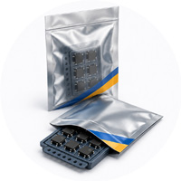
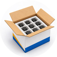
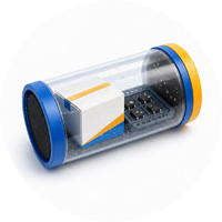
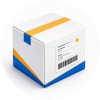
Packaging and Shipping Protection

Step 1 product inspection
Step 1 Product Inspection
Step 2 casing and dry pipe protection
Step 2 Casing & Dry Pipe
Step 3 anti-static bag packaging
Step 3 Anti-static Bags
Step 4 inner carton packaging
Step 4 Inner Carton
Step 5 shipping label
Step 5 Shipping Label
Step 6 international delivery
Step 6 International Delivery

Packaging may be adjusted according to product type, quantity, moisture sensitivity and destination requirements.

Related Products

TPS562201DDCR Texas Instruments
TPS562201DDCR

Texas Instruments

MC34063ABD-TR STMicroelectronics
MC34063ABD-TR

STMicroelectronics

TPS561201DDCR Texas Instruments
TPS561201DDCR

Texas Instruments

MC33063ADR Texas Instruments
MC33063ADR

Texas Instruments

MC34063ADR Texas Instruments
MC34063ADR

Texas Instruments

TPS560200DBVR Texas Instruments
TPS560200DBVR

Texas Instruments

AP3012KTR-G1 Diodes Incorporated
AP3012KTR-G1

Diodes Incorporated

TLV61048DBVR Texas Instruments
TLV61048DBVR

Texas Instruments

AZ34063UMTR-G1 Diodes Incorporated
AZ34063UMTR-G1

Diodes Incorporated

TPS562200DDCR Texas Instruments
TPS562200DDCR

Texas Instruments

AP62300TWU-7 Diodes Incorporated
AP62300TWU-7

Diodes Incorporated

MC34063EBD-TR STMicroelectronics
MC34063EBD-TR

STMicroelectronics

SOURCING SUPPORT

LT8365JMSE#TRPBF Procurement and Technical Support

LT8365JMSE#TRPBF is manufactured by Analog Devices Inc.. This page provides purchasing information including manufacturer, category, package, datasheet, stock reference, price reference and product specifications.

Haishengye Electronics supports customers sourcing LT8365JMSE#TRPBF and related electronic components for prototype development, maintenance, NPI, production preparation and one-stop BOM procurement.

Submit an RFQ to request the latest stock, price, lead time, batch information, alternative parts, package confirmation or technical documents for LT8365JMSE#TRPBF.

Part Number
LT8365JMSE#TRPBF
Manufacturer
Analog Devices Inc.
Package
16-TFSOP (0.118", 3.00mm Width), 12 Leads, Exposed Pad
Category
Voltage Regulators - DC DC Switching Regulators
Submitting...
Please wait while we submit your inquiry.

Tips

Please check your information and try again.