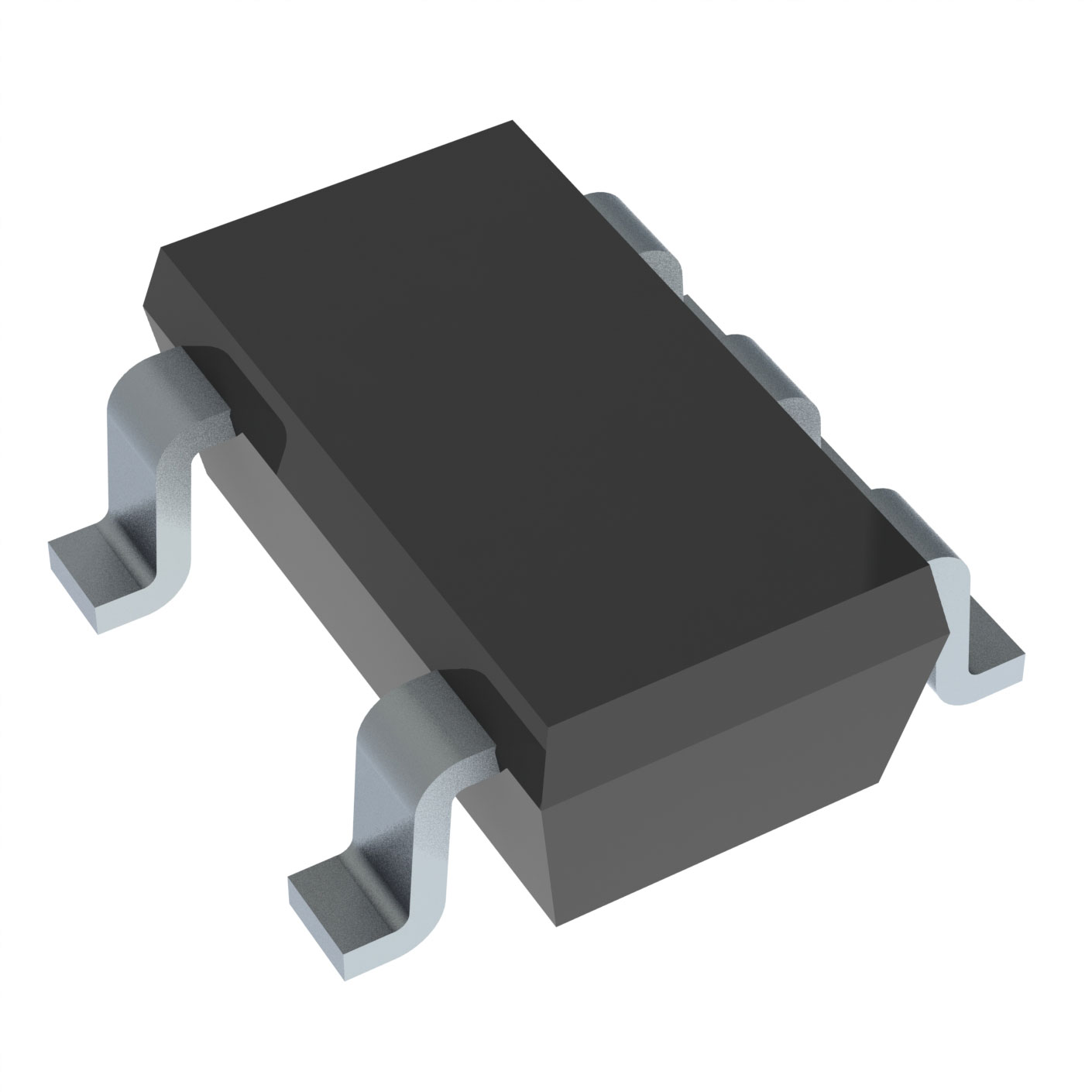
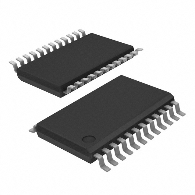
SN74LVC8T245MPWREP is an Enhanced Product 8-bit non-inverting dual-supply bus transceiver from Texas Instruments that uses two separate configurable power-supply rails. The A port is designed to track VCCA, which accepts any supply voltage from 1.65V to 5.5V. The B port is designed to track VCCB, which also accepts any supply voltage from 1.65V to 5.5V. This allows for universal low-voltage bidirectional translation between any of the 1.8V, 2.5V, 3.3V, and 5.5V voltage nodes.
The SN74LVC8T245MPWREP is designed for asynchronous communication between two data buses. The logic levels of the direction-control (DIR) input and the output-enable (OE) input activate either the B-port outputs or the A-port outputs or place both output ports into the high-impedance mode. The device transmits data from the A bus to the B bus when the B-port outputs are activated, and from the B bus to the A bus when the A-port outputs are activated. The input circuitry on both A and B ports is always active and must have a logic HIGH or LOW level applied to prevent excess ICC and ICCZ.
The device is designed so that the control pins (DIR and OE) are supplied by VCCA. It is fully specified for partial-power-down applications using Ioff, which disables the outputs to prevent damaging current backflow through the device when it is powered down. The VCC isolation feature ensures that if either VCC input is at GND, all outputs are in the high-impedance state. To ensure the high-impedance state during power up or power down, OE should be tied to VCC through a pullup resistor.
The SN74LVC8T245MPWREP is an Enhanced Product grade device featuring a controlled baseline, one assembly/test site, one fabrication site, extended product life cycle, extended product-change notification, and product traceability. It is available in a 24-pin TSSOP package with a 4.40mm × 7.80mm body size, rated for operation from –55°C to +125°C. The device is RoHS compliant, REACH unaffected, and in active production.
Fully Configurable Dual-Rail Design Each port operates over the full 1.65V to 5.5V power-supply range, enabling universal low-voltage bidirectional translation between 1.8V, 2.5V, 3.3V, and 5.5V nodes.
VCC Isolation & Ioff Support If either VCC input is at GND, all outputs are in the high-impedance state. Ioff circuitry disables outputs during partial-power-down, preventing damaging current backflow.
Enhanced Product Grade Controlled baseline, one assembly/test site, one fabrication site, extended product life cycle, extended product-change notification, and product traceability with –55°C to +125°C operation.