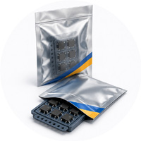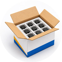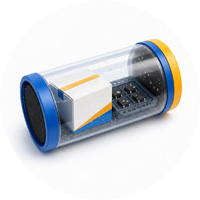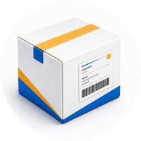
Professional testing equipment and reports to ensure product quality.
Analog Devices Inc. RFQ AVAILABLE

ADRF5720BCCZN-R7

0.5DB LSB,6-BIT,SILICON DIGITAL

Part Number
ADRF5720BCCZN-R7
Manufacturer
Analog Devices Inc.
Category
Attenuators
Package
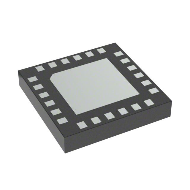
24-VFLGA Exposed Pad
Datasheet:
ADRF5720BCCZN-R7.pdf
Description
0.5DB LSB,6-BIT,SILICON DIGITAL
Select Quantity Stock: 2,684

FAST RESPONSE

Quick RFQ

Send your requirements and our sales team will contact you as soon as possible.

Part Number
Quantity *
Target Price
Name *
Company *
Email *
Comments
PRODUCT INFORMATION

Product Details

PRODUCT TECHNICAL REFERENCE

ADRF5720BCCZN-R7 0.5 dB LSB, 6-Bit, Silicon Digital Attenuator, 9 kHz to 40 GHz

A comprehensive technical overview of the ADRF5720BCCZN-R7, an ultrawideband 6-bit silicon digital attenuator from Analog Devices featuring a 9 kHz to 40 GHz frequency range, 31.5 dB attenuation control range in 0.5 dB steps, low insertion loss of 2.0 dB up to 18 GHz and 4.5 dB up to 40 GHz, high RF input power handling of 27 dBm average and 30 dBm peak, SPI and parallel mode control, and a 24-terminal 4 mm × 4 mm LGA package. Covers device function, core features, electrical specifications, pin configuration, typical applications, and replacement selection guidance.

Analog Devices 24-Terminal LGA (4mm × 4mm) 9 kHz to 40 GHz
Device Classification 6-Bit Silicon Digital Attenuator
Part Number
ADRF5720BCCZN-R7
Mounting Type
Surface Mount
Operating Temperature Range
-40°C to +105°C
01
PRODUCT OVERVIEW

What Is the ADRF5720BCCZN-R7?

ADRF5720BCCZN-R7 is an ultrawideband, high-precision 6-bit silicon digital attenuator from Analog Devices that operates from 9 kHz to 40 GHz with a 31.5 dB attenuation control range in 0.5 dB steps. The device provides better than 4.5 dB of insertion loss and excellent attenuation accuracy, making it ideal for demanding RF and microwave applications.

The ADRF5720 handles a maximum input power of 27 dBm average and 30 dBm peak for all states, with high input linearity (P0.1dB of 30 dBm in insertion loss state, 27 dBm in other attenuation states; IP3 of 50 dBm typical). The ATTIN and ATTOUT ports are internally matched to 50 Ω and DC-coupled to 0 V, eliminating the need for DC blocking capacitors when the RF line potential is equal to 0 V DC.

The device requires a dual supply voltage of +3.3 V and −3.3 V and features serial peripheral interface (SPI), parallel mode control, and CMOS/LVTTL-compatible controls. The ADRF5720 is pin-compatible with the ADRF5730, the fast switching version, which operates from 100 MHz to 40 GHz. The device is available in a 24-terminal, 4 mm × 4 mm, RoHS-compliant land grid array (LGA) package and operates from –40°C to +105°C.

Ultrawideband 9 kHz to 40 GHz 31.5 dB attenuation control range in 0.5 dB steps with low insertion loss of 2.0 dB up to 18 GHz and 4.5 dB up to 40 GHz.
High RF Power Handling 27 dBm average and 30 dBm peak input power handling for all states, with high input linearity (IP3 of 50 dBm typical).
SPI and Parallel Control CMOS/LVTTL-compatible serial and parallel control interfaces with RF amplitude settling time of 8 µs and no low frequency spurious signals.
02
DEVICE HIGHLIGHTS

Key Features and Benefits of ADRF5720BCCZN-R7

Ultrawideband Frequency Range (9 kHz to 40 GHz)

Operates from 9 kHz to 40 GHz, covering a broad spectrum of RF and microwave applications including 5G millimeter wave, military radios, radars, and VSATs.

6-Bit Attenuation Control (0.5 dB Steps)

31.5 dB attenuation control range in 0.5 dB steps with excellent attenuation accuracy: ±(0.20 + 1.0% of attenuation state) up to 18 GHz, ±(0.20 + 1.5%) up to 26 GHz, ±(0.40 + 3.0%) up to 40 GHz.

High Input Power Handling

ATTIN port handles 27 dBm average and 30 dBm peak RF input power for all states, with P0.1dB of 30 dBm (insertion loss state) and 27 dBm (other attenuation states).

SPI and Parallel Mode Control

Features serial peripheral interface (SPI), parallel mode control, and CMOS/LVTTL-compatible controls for flexible system integration.

Fast RF Settling Time (8 µs)

RF amplitude settling time of 8 µs to 0.1 dB of final RF output, enabling rapid attenuation switching in time-critical applications.

Compact 24-Terminal LGA Package

24-terminal, 4 mm × 4 mm land grid array (LGA) package with exposed pad, RoHS compliant and pin-compatible with the ADRF5730 fast switching version.

03
REFERENCE DATA

Technical Specifications for ADRF5720BCCZN-R7

Part Number ADRF5720BCCZN-R7 Manufacturer Analog Devices
Device Type 6-Bit Silicon Digital Attenuator Attenuation Range 31.5 dB in 0.5 dB Steps
Frequency Range 9 kHz to 40 GHz Insertion Loss 2.0 dB (up to 18 GHz), 2.8 dB (up to 26 GHz), 4.5 dB (up to 40 GHz)
Attenuation Accuracy ±(0.20 + 1.0%) up to 18 GHz; ±(0.20 + 1.5%) up to 26 GHz; ±(0.40 + 3.0%) up to 40 GHz Step Error (Typical) ±0.25 dB up to 26 GHz; ±0.65 dB up to 40 GHz
P0.1dB (Insertion Loss State) 30 dBm P0.1dB (Other Attenuation States) 27 dBm
IP3 (Typical) 50 dBm RF Input Power Handling 27 dBm Average, 30 dBm Peak (All States)
Supply Voltage (VDD) +3.3 V Supply Voltage (VSS) −3.3 V
Control Interface SPI, Parallel Mode, CMOS/LVTTL Compatible RF Settling Time (0.1 dB) 8 µs
Impedance 50 Ω (Internal Match) DC Coupling ATTIN and ATTOUT DC-Coupled to 0 V
Package / Case 24-Terminal LGA (4 mm × 4 mm × 0.75 mm) Supplier Device Package LGA-24 (CC-24-5)
Exposed Pad 2.4 mm EP (Must Be Connected to RF and DC Ground) Pin Count 24 (Plus Exposed Pad)
Mounting Type Surface Mount Operating Temperature -40°C to +105°C
ESD Rating (HBM) Class 1B (1000 V) RoHS ROHS3 Compliant
REACH Status REACH Unaffected MSL Level MSL 3 (168 Hours)
ECCN EAR99 HTSUS 8542.39.0070
Product Status Active Packaging Tape & Reel (500 per Reel)
Pin-Compatible With ADRF5730 (Fast Switching Version, 100 MHz to 40 GHz) Evaluation Board ADRF5720-EVALZ

Electrical values shown above are reference values. Test conditions, limits, and guaranteed performance should always be confirmed from the current official manufacturer datasheet before design or production use.

04
DESIGN REFERENCE

Circuit Considerations for ADRF5720BCCZN-R7

Control Interface & Attenuation Programming

The ADRF5720BCCZN-R7 offers flexible control interface and attenuation programming:

  • Parallel Mode (PS = Low): The six attenuation bits are controlled directly by pins D0 (0.5 dB), D1 (1 dB), D2 (2 dB), D3 (4 dB), D4 (8 dB), and D5 (16 dB). Latch Enable (LE) latches the parallel data.
  • Serial Mode (PS = High): The SPI interface uses SERIN (serial data input), CLK (serial clock), and LE (latch enable) to shift in the 6-bit attenuation word. SEROUT provides serial data output for daisy-chain operation.
  • Control Pin Compatibility: All digital inputs (LE, PS, D3/SEROUT, D4/SERIN, D5/CLK) are CMOS/LVTTL compatible. D0, D1, and D2 have internal 100 kΩ pull-up resistors.
  • Attenuation Word: The 6-bit binary word sets attenuation from 0 dB (000000) to 31.5 dB (111111) in 0.5 dB steps.

PCB and System-Level Guidance

Attenuator performance depends on layout and component selection:

  • Power Supply Decoupling: Place low-ESR decoupling capacitors close to the VDD and VSS pins for stable dual-supply operation (+3.3 V and −3.3 V).
  • RF Ports (ATTIN and ATTOUT): Both ports are internally DC-coupled to 0 V and AC-matched to 50 Ω. No DC blocking capacitors are necessary when the RF line potential is equal to 0 V DC.
  • Exposed Pad: The exposed pad (EP) must be connected to the RF and DC ground of the PCB for optimal performance and thermal dissipation.
  • Impedance Matching: For wideband applications, impedance matching on the RF transmission lines can further optimize high frequency insertion loss, return loss, and attenuation accuracy characteristics. Optimal footprint and land pattern design improves attenuation accuracy above 35 GHz.
  • Ground Vias: Use multiple ground vias near the GND pins and exposed pad to minimize parasitic inductance and ensure a low-impedance ground return path.
  • Verify the recommended PCB footprint from the official datasheet prior to production.
05
24-TERMINAL LGA (4 mm × 4 mm)

Pin Configuration Reference for ADRF5720BCCZN-R7

ADRF5720
LGA TOP VIEW

Confirm package orientation and pin numbering against the official package drawing before PCB layout. The LGA package has 24 terminals with a 4 mm × 4 mm body size and 0.75 mm package height. The exposed pad (2.4 mm) must be connected to the RF and DC ground of the PCB.

1 LE Latch Enable Input - Latches Parallel Data or Serial Data
2 PS Parallel/Serial Control Interface Selection - Low = Parallel, High = Serial
3 GND Ground - Connect to RF and DC Ground
4 GND Ground - Connect to RF and DC Ground
5 ATTIN Attenuator Input - DC-Coupled to 0 V, AC-Matched to 50 Ω
6 GND Ground - Connect to RF and DC Ground
7 GND Ground - Connect to RF and DC Ground
8 GND Ground - Connect to RF and DC Ground
9 GND Ground - Connect to RF and DC Ground
10 GND Ground - Connect to RF and DC Ground
11 GND Ground - Connect to RF and DC Ground
12 GND Ground - Connect to RF and DC Ground
13 GND Ground - Connect to RF and DC Ground
14 ATTOUT Attenuator Output - DC-Coupled to 0 V, AC-Matched to 50 Ω
15 GND Ground - Connect to RF and DC Ground
16 GND Ground - Connect to RF and DC Ground
17 VSS Negative Supply Input - −3.3 V
18 VDD Positive Supply Input - +3.3 V
19 D0 Parallel Control Input - 0.5 dB Attenuator Bit (Internal 100 kΩ Pull-Up)
20 D1 Parallel Control Input - 1 dB Attenuator Bit (Internal 100 kΩ Pull-Up)
21 D2 Parallel Control Input - 2 dB Attenuator Bit (Internal 100 kΩ Pull-Up)
22 D3/SEROUT Parallel Control Input - 4 dB Bit / Serial Data Output (SEROUT)
23 D4/SERIN Parallel Control Input - 8 dB Bit / Serial Data Input (SERIN)
24 D5/CLK Parallel Control Input - 16 dB Bit / Serial Clock Input (CLK)
EP EPAD Exposed Pad - Must Be Connected to RF and DC Ground of PCB
06
APPLICATION AREAS

Typical Applications for ADRF5720BCCZN-R7

Test and Instrumentation

Ultrawideband 9 kHz to 40 GHz frequency range and high attenuation accuracy make this attenuator ideal for precision test and measurement equipment.

Cellular Infrastructure: 5G Millimeter Wave

Supports 5G millimeter wave infrastructure with high linearity (IP3 of 50 dBm typical) and low insertion loss across the wide frequency range.

Military Radios, Radars, ECMs

High RF input power handling (27 dBm average, 30 dBm peak) and robust ESD protection suit military radios, radars, and electronic counter measures.

Microwave Radios and VSATs

Low insertion loss and tight distribution in relative phase enable precise signal level control in microwave radios and very small aperture terminals.

Industrial Scanners

Wide frequency range and fast RF settling time (8 µs) support industrial scanning and imaging applications.

Wideband RF Signal Chains

Pin-compatible with the ADRF5730 fast switching version for design flexibility, and suitable for wideband RF signal chain applications requiring precise attenuation control.

07
REPLACEMENT GUIDANCE

Selecting an Alternative for ADRF5720BCCZN-R7

A replacement for the ADRF5720BCCZN-R7 should not be selected solely by product category. The electrical characteristics, package, and pin configuration must be evaluated against the specific circuit requirements. The following alternatives are documented in the official Analog Devices product pages and datasheets.

Type: 6-Bit Silicon Digital Attenuator
Frequency range: 9 kHz–40 GHz
Attenuation range: 0.5–31.5 dB
Step size: 0.5 dB
Insertion loss: 4.5 dB up to 40 GHz
Package: 24-Terminal LGA
Temperature range: –40°C to 105°C
SPI and parallel control

Pin-compatible and functionally compatible alternatives (same family):

Part Number Frequency Range Package Key Difference
ADRF5720BCCZN-R7 9 kHz to 40 GHz 24-LGA (4 mm × 4 mm) -
ADRF5730BCCZN-R7 100 MHz to 40 GHz 24-LGA (4 mm × 4 mm) Pin-Compatible, Fast Switching Version
ADRF5721BCCZN-R7 9 kHz to 40 GHz 24-LGA (4 mm × 4 mm) Different Attenuation Range / Feature Set

All alternative part numbers listed above are documented in the official Analog Devices product pages and datasheets. The ADRF5720BCCZN-R7 is the standard switching version in a 24-terminal LGA package with tape-and-reel packaging (500 units per reel). For the fast switching version that is pin-compatible and operates from 100 MHz to 40 GHz, consider ADRF5730BCCZN-R7. For a different attenuation range or feature set, consider ADRF5721BCCZN-R7. Select based on switching speed, frequency range, and application requirements.

Alternative Part Support

Send the original part number, application, required quantity, and key parameters to Haishengye Electronics for replacement-part sourcing support.

Ask About Alternatives
MANUFACTURER INFORMATION

Analog Devices

The ADRF5720 (ADRF5720BCCZN-R7) belongs to the family of ultrawideband silicon digital attenuators from Analog Devices. The device is a 6-bit digital attenuator with a 31.5 dB attenuation control range in 0.5 dB steps, operating from 9 kHz to 40 GHz. The ADRF5720 features low insertion loss, excellent attenuation accuracy, high input linearity, and high RF input power handling. The device requires a dual supply voltage of +3.3 V and −3.3 V and supports SPI and parallel mode control with CMOS/LVTTL-compatible interfaces. The ADRF5720 is pin-compatible with the ADRF5730 fast switching version and is available in a 24-terminal, 4 mm × 4 mm, RoHS-compliant LGA package operating from −40°C to +105°C. The device is recommended for new designs in test and instrumentation, 5G millimeter wave infrastructure, military radios, radars, ECMs, microwave radios, and VSAT applications.

SUPPLIED BY

Haishengye Electronics

Haishengye Electronics provides electronic component stock supply, BOM sourcing, quotation support, and quality inspection services for ADRF5720BCCZN-R7 and related devices.

Submit Your Requirements
Technical Information Disclaimer

This technical guide is provided for product identification and preliminary reference only. Electrical limits, package dimensions, pin configuration, product status, and application suitability must be verified using current official manufacturer documentation before design, procurement, or production.

TECHNICAL RESOURCES

ADRF5720BCCZN-R7 Technical Information

  • Specifications
  • FAQ
  • Hot Sale
  • Packaging
  • Related Products

Specifications

Product Attribute
Attribute Value
Part Number
ADRF5720BCCZN-R7
Manufacturer
Analog Devices Inc.
Package
24-VFLGA Exposed Pad
Package/Case
24-VFLGA Exposed Pad
Series
ADRF5720
Packaging
Tape & Reel (TR) Cut Tape (CT) Digi-Reel®
Product Status
Active
Attenuation Value
0.5dB ~ 31.5dB
Frequency Range
9 kHz ~ 40 GHz
Power (Watts)
500mW
Impedance
50 Ohms
Grade
-
Qualification
-

Frequently Asked Questions

1. How can I order ADRF5720BCCZN-R7 from Haishengye Electronics?

Submit an RFQ directly on this page with your required quantity, target price and delivery requirements. Our sales team will review the request and provide a quotation.

2. How does Haishengye Electronics verify the quality of ADRF5720BCCZN-R7?

We work with qualified suppliers and review sourcing channels, traceability, packaging and product condition before shipment.

3. Are the stock and price of ADRF5720BCCZN-R7 updated in real time?

Electronic component inventory and prices may change frequently. Displayed values are references, and final stock and pricing will be confirmed in the quotation.

4. Which payment methods are supported?

Wire Transfer, PayPal, Alipay, WeChat, Credit Card, Western Union, MoneyGram and Escrow may be supported depending on the order and destination.

5. How is international shipping arranged?

International shipping may be arranged through DHL, UPS, FedEx, TNT and other logistics channels. Tracking information will be provided after shipment.

6. What is the return or replacement process for ADRF5720BCCZN-R7?

Contact our sales team within the agreed period if there are quantity differences, incorrect items or clear external defects. Products should remain unused and in their original packaging.

7. Can I request technical support for ADRF5720BCCZN-R7?

Yes. Contact our team for datasheets, package details, product specifications, alternative parts and sourcing assistance.

Packaging and Shipping Protection

Step 1 product inspection
Step 1 Product Inspection
Step 2 casing and dry pipe protection
Step 2 Casing & Dry Pipe
Step 3 anti-static bag packaging
Step 3 Anti-static Bags
Step 4 inner carton packaging
Step 4 Inner Carton
Step 5 shipping label
Step 5 Shipping Label
Step 6 international delivery
Step 6 International Delivery

Packaging may be adjusted according to product type, quantity, moisture sensitivity and destination requirements.

Related Products

ADRF5720BCCZN-R7 Analog Devices Inc.
ADRF5720BCCZN-R7

Analog Devices Inc.

SOURCING SUPPORT

ADRF5720BCCZN-R7 Procurement and Technical Support

ADRF5720BCCZN-R7 is manufactured by Analog Devices Inc.. This page provides purchasing information including manufacturer, category, package, datasheet, stock reference, price reference and product specifications.

Haishengye Electronics supports customers sourcing ADRF5720BCCZN-R7 and related electronic components for prototype development, maintenance, NPI, production preparation and one-stop BOM procurement.

Submit an RFQ to request the latest stock, price, lead time, batch information, alternative parts, package confirmation or technical documents for ADRF5720BCCZN-R7.

Part Number
ADRF5720BCCZN-R7
Manufacturer
Analog Devices Inc.
Package
24-VFLGA Exposed Pad
Category
Attenuators
Submitting...
Please wait while we submit your inquiry.

Tips

Please check your information and try again.