
1. What Is an Analog-to-Digital Converter (ADC)?
An analog-to-digital converter (ADC) is an integrated circuit that transforms a continuously varying analog signal-such as voltage, current, or temperature-into a discrete digital code that processors, microcontrollers, and DSPs can process, store, and transmit. Without ADCs, the digital revolution would be impossible: every sensor reading, every audio recording, every medical image begins with an analog signal that must be digitized.
The fundamental operation of an ADC involves two distinct processes: sampling and quantization. Sampling discretizes the signal in the time domain, converting a continuous-time signal into a discrete-time signal at a specific sampling frequency (fs). Quantization then discretizes the signal in the amplitude domain, mapping each sample to the nearest of 2N discrete levels, where N is the ADC resolution in bits[reference:0].
In practice, the sampling operation is performed by a sample-and-hold (S/H) circuit, which captures the instantaneous analog value and holds it steady long enough for the quantizer to produce a correct result[reference:1]. The quantizer then represents each sample in binary form with a finite word length-for a 16-bit ADC, that means 65,536 possible output codes.
2. Core Principles: Sampling and Quantization
Understanding ADC operation requires a firm grasp of the two fundamental processes that define conversion accuracy and speed.
2.1. Sampling and the Nyquist Theorem
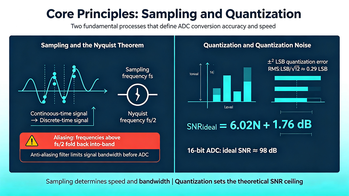
The sampling process converts a continuous-time signal into a discrete-time signal at regular intervals defined by the sampling frequency. The Nyquist-Shannon sampling theorem states that an input signal must be sampled at least twice as fast as the highest frequency component of interest to avoid aliasing[reference:3]. If the signal contains frequencies above half the sampling rate (the Nyquist frequency), those frequencies will fold back into the in-band spectrum as false components-a phenomenon called aliasing that is irreversible once it occurs.
To satisfy the Nyquist criterion, an anti-aliasing filter (typically a low-pass analog filter) is placed before the ADC to restrict the signal bandwidth[reference:4]. The filter must attenuate frequencies above fs/2 to below the ADC's noise floor, ensuring that aliased components do not corrupt the digitized signal.
2.2. Quantization and Quantization Noise
Quantization maps each sampled value to the nearest discrete output code. Because the analog input has infinite precision while the digital output has finite resolution, an inherent error called quantization error is introduced. For an ideal ADC, the quantization error amplitude is ±½ LSB, with an RMS value of LSB/√12 ≈ 0.29 LSB[reference:5].
The quantization error manifests as quantization noise-an irreversible corruption of the signal that establishes the theoretical maximum signal-to-noise ratio (SNR) for an ideal N-bit converter:
SNRideal = 6.02N + 1.76 dB
This formula represents the fundamental performance ceiling for any ADC with N-bit resolution. A 16-bit ADC, for example, has an ideal SNR of approximately 98 dB-but as discussed in Section 4, real-world performance rarely achieves this theoretical maximum[reference:6].
3. Main ADC Architectures
ADC architectures occupy different regions of the speed-resolution trade-off space. No single architecture wins everywhere-each involves fundamental trade-offs between conversion speed, resolution, power consumption, and silicon area. Understanding these trade-offs is essential for selecting the right ADC for a given application.
| Architecture | Resolution Range | Speed Range | Key Characteristics | Best Use Case |
|---|---|---|---|---|
| SAR (Successive Approximation Register) | 8–18 bits | Up to ~5 MSPS | Zero pipeline latency; power scales linearly with sampling rate | Closed-loop control, motor drives, multiplexed data acquisition |
| Delta-Sigma (ΔΣ) | 16–32 bits | DC to a few MHz | Oversampling and noise shaping; relaxed anti-aliasing requirements; conversion latency | Precision instrumentation, medical, audio, seismic sensing |
| Pipelined | 8–16 bits | MSPS to GSPS | Multi-stage conversion; high throughput at moderate power | Communications, radar, high-speed data acquisition |
| Flash | 4–8 bits | GSPS range | 2N−1 parallel comparators; fastest but most power- and area-intensive | High-speed oscilloscopes, direct RF sampling |
3.1. SAR ADC: The Workhorse of Medium-Speed Acquisition
The Successive Approximation Register (SAR) ADC executes a binary search algorithm using an internal capacitive DAC and a single comparator[reference:7]. For an N-bit converter, the conversion completes within N clock cycles-typically 13 conversion cycles for a 12-bit ADC like the one specified in TI's TMS570 microcontroller datasheet[reference:8].
SAR ADCs offer three core advantages: zero pipeline latency (data is available immediately after the conversion cycle), power scaling (consumption scales linearly with sampling rate), and a broad resolution envelope from 8 to 20 bits[reference:9]. These characteristics make SAR ADCs optimal for closed-loop control systems, motor drives, and rapid multi-channel multiplexing.
A representative example is the 16-bit, 5 MSPS SAR ADC IP core from T2M, which achieves 82 dB SNDR, −92 dB THD, and 13.5 ENOB, with built-in offset and gain calibration that compensates for voltage, temperature, and process variations[reference:10].
3.2. Delta-Sigma ADC: Precision at Low Speed
Delta-sigma (ΔΣ) converters combine oversampling, noise shaping, and digital decimation filtering to push quantization noise outside the signal band of interest[reference:11]. This architecture achieves the highest dynamic range of any ADC type-16-bit to 32-bit resolution across bandwidths from DC to a few megahertz[reference:12].
Because the effective sampling rate occurs at the oversampled modulator clock (fmod = OSR × fs), the Nyquist zone is shifted higher in frequency, allowing simple first- or second-order passive RC anti-aliasing filters rather than sharp analog filters[reference:13]. However, the internal digital decimation filter introduces multi-cycle group delay, making delta-sigma ADCs less suitable for fast multiplexed inputs or real-time closed-loop feedback paths[reference:14].
3.3. Pipelined and Flash ADCs: Speed Above All
Pipelined ADCs divide the quantization process into multiple consecutive stages, each resolving a few bits and passing a residue to the next stage[reference:15]. This architecture achieves high throughput at moderate power consumption, making it the standard choice for communications, radar, and high-speed data acquisition systems.
Flash ADCs use 2N−1 parallel comparators to resolve an N-bit output in a single clock cycle-the fastest architecture available, but also the most area- and power-intensive[reference:16]. Flash converters are typically limited to 4–8 bits and are used primarily in high-speed oscilloscopes and direct RF sampling applications.
4. Key Specifications for ADC Selection
Selecting an ADC based solely on nameplate resolution and sampling rate frequently leads to compromised performance. A nominal 16-bit converter can easily degrade to 11 ENOB if front-end settling, reference noise, or clock phase noise are improperly budgeted[reference:17]. The following parameters are essential for informed selection.
4.1. Resolution vs. Effective Number of Bits (ENOB)
Resolution specifies the number of output bits an ADC produces-a 16-bit ADC outputs 216 = 65,536 codes. However, Effective Number of Bits (ENOB) represents the actual usable resolution after accounting for noise and distortion:
ENOB = (SINAD − 1.76) / 6.02
where SINAD is the Signal-to-Noise-and-Distortion ratio[reference:18]. A 16-bit ADC with 82 dB SNR and −90 dB THD may deliver only 13.3 ENOB-a full 2.7 bits below its nameplate resolution[reference:19].
This gap between nameplate and actual performance underscores a critical selection principle: buy ENOB, not resolution. The ideal SNR formula (6.02N + 1.76 dB) is a ceiling, not a promise-the reference, clock, and board layout determine how many of those bits are real[reference:20].
4.2. Key Dynamic and DC Specifications
| Parameter | Definition | Typical Values (12-bit ADC) |
|---|---|---|
| SNR (Signal-to-Noise Ratio) | Ratio of signal power to noise power (excluding harmonics) | 70 dB (at 200 kHz, −0.5 dBFS) |
| THD (Total Harmonic Distortion) | Ratio of harmonic components to fundamental signal | −75 dB |
| SINAD | Signal-to-noise-and-distortion ratio (noise + harmonics) | 69 dB |
| INL (Integral Nonlinearity) | Maximum deviation from ideal transfer function | ±2 LSB |
| DNL (Differential Nonlinearity) | Deviation of code width from ideal 1 LSB | ±1 LSB |
| Offset Error | Deviation of actual zero-code transition from ideal | ±5 LSB |
| Gain Error | Deviation of actual full-scale transition from ideal | ±10 LSB |
These specifications are drawn from the TI TMS570 microcontroller datasheet, which specifies a 12-bit ADC with SNR of 70 dB, THD of −75 dB, and INL/DNL within ±2 LSB and ±1 LSB respectively[reference:21].
5. Application of Analog-to-Digital Converter Across Industries
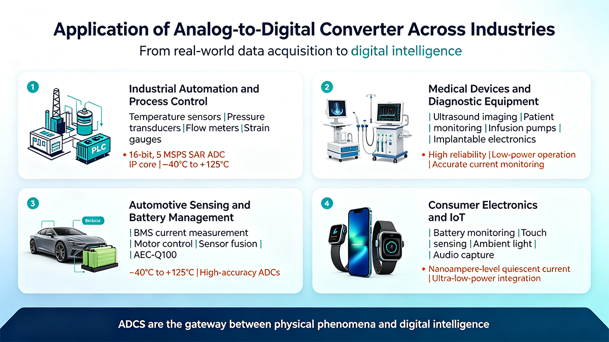
The application of analog to digital converter spans virtually every industry that relies on real-world data acquisition. From factory floors to hospital operating rooms to electric vehicle battery packs, ADCs are the gateway between physical phenomena and digital intelligence.
5.1. Industrial Automation and Process Control
In industrial environments, ADCs digitize signals from temperature sensors, pressure transducers, flow meters, and strain gauges. Modern industrial systems require isolated ADCs and amplifiers for PLCs and motor drives, handling wide dynamic ranges and harsh operating conditions[reference:22][reference:23]. The 16-bit, 5 MSPS SAR ADC IP core is highly suited for industrial automation, robotics, and precision instrumentation, qualified for −40°C to +125°C operation[reference:24].
5.2. Medical Devices and Diagnostic Equipment
Medical applications impose some of the most demanding ADC requirements. In ultrasound imaging, the ADC is a critical building block in the receive chain, enabling digital beamforming and image reconstruction[reference:25]. Patient monitoring systems, infusion pumps, and implantable electronics require extremely reliable signal conversion to ensure correct operation and patient safety[reference:26]. For low-power biomedical implants, accurate current monitoring enables precise control of stimulation signals and prolongs battery life[reference:27].
5.3. Automotive Sensing and Battery Management
Automotive systems depend on high-accuracy ADCs for battery management, motor control, and sensor fusion. Precision current measurement is essential for electric vehicle battery management systems, where small current variations carry meaningful information about state of charge and battery health[reference:28]. Automotive-qualified ADCs must operate across −40°C to +125°C and meet AEC-Q100 reliability standards[reference:29].
5.4. Consumer Electronics and IoT
In consumer devices, ADCs enable battery monitoring, touch sensing, ambient light detection, and audio capture. Low-power IoT sensor nodes rely on ADCs with nanoampere-level quiescent currents to extend battery life[reference:30]. The integrate-and-fire ADC architecture-which converts current into a frequency-domain pulse signal-is particularly well-suited for ultra-low-power battery monitoring and high-density integration scenarios[reference:31].
6. ADC Selection and Design Considerations
A successful ADC design extends beyond component selection. The following considerations address the system-level factors that determine whether a converter achieves its datasheet performance in practice.
6.1. Clock Jitter: The Hidden SNR Killer
Clock jitter introduces timing uncertainty in the sampling instant, degrading SNR in a frequency-dependent manner. At a 10 MHz input frequency, just 200 fs of jitter caps SNR near 98 dB-effectively erasing the performance advantage of a 16-bit converter[reference:32]. This relationship makes clock source selection critical for high-speed, high-resolution applications.
6.2. Reference Noise and Stability
The ADC reference voltage establishes the conversion scale-any noise or drift on the reference directly translates to conversion error. Reference noise contributes to the overall noise floor, reducing ENOB. For precision applications, a low-noise, low-drift voltage reference with appropriate decoupling is essential[reference:33].
6.3. Mixed-Signal PCB Layout
Mixed-signal PCB layout requires physical separation of analog and digital domains with a unified ground plane connected at a single point beneath the ADC[reference:34]. Key practices include:
- Separate analog and digital signal routing: Keep high-speed digital traces away from sensitive analog inputs[reference:35].
- Guard traces and ground fill: Fill void areas on signal layers with ground fill and use guard traces around analog input traces[reference:36].
- Single-point grounding: Connect analog and digital ground planes at a single point beneath the ADC to prevent ground loops[reference:37].
- Decouple the reference: Place low-ESR ceramic capacitors close to the reference pin to suppress high-frequency noise.
7. ADC Selection Checklist
- Define signal bandwidth and required sampling rate (must be ≥ 2× the highest signal frequency for Nyquist compliance).
- Determine required ENOB based on accuracy needs-not nameplate resolution.
- Select architecture: SAR for medium-speed multiplexed acquisition, delta-sigma for high-resolution precision, pipelined/flash for high-speed.
- Verify input voltage range matches the signal conditioning output and reference voltage.
- Evaluate SNR, THD, and SINAD specifications against application requirements.
- Check INL and DNL for linearity requirements-critical for precision measurement.
- Select an anti-aliasing filter that attenuates out-of-band signals below the ADC noise floor.
- Evaluate clock jitter requirements-at high input frequencies, femtosecond-level jitter degrades SNR.
- Confirm interface compatibility (SPI, I²C, LVDS, JESD204B/C) with the host processor.
- Follow mixed-signal PCB layout guidelines: separate analog/digital domains, single-point grounding, guard traces.
8. Frequently Asked Questions (FAQ)
Resolution is the number of bits the ADC outputs (e.g., 16-bit). ENOB (Effective Number of Bits) is the actual usable resolution after accounting for noise and distortion, calculated as ENOB = (SINAD − 1.76) / 6.02. A 16-bit ADC may only deliver 12–13 ENOB in practice.
Choose SAR ADCs for medium-speed multiplexed acquisition (8–18 bit, up to ~5 MSPS). Choose delta-sigma ADCs for high-resolution, low-speed precision measurement (16–32 bit). Choose pipelined or flash ADCs for high-speed applications (MSPS to GSPS).
The Nyquist theorem states that an input signal must be sampled at least twice as fast as its highest frequency component. Sampling below this rate causes aliasing-high-frequency signals appearing as false lower-frequency components. An anti-aliasing filter before the ADC prevents this.
Clock jitter introduces timing uncertainty in the sampling instant, degrading SNR. At a 10 MHz input frequency, just 200 fs of jitter caps SNR near 98 dB-effectively erasing the performance advantage of a 16-bit converter.
ADCs are used in industrial automation and process control, medical diagnostic equipment (ultrasound, patient monitoring), automotive sensing and battery management, precision instrumentation, audio recording, and IoT sensor nodes for converting real-world analog signals into digital data.
9. Industry Trends and Outlook
ADC technology continues to evolve to meet the demands of increasingly digital, sensor-rich systems. Key trends shaping the industry include:
- Hybrid architectures: The trend of hybrid ADC design extends beyond the choice of quantizer to include a mix of circuit topologies in key building blocks, leading to performance levels beyond what conventional architectures achieve[reference:38].
- Digital calibration and correction: On-chip digital logic that compensates for analog imperfections-such as comparator offset and capacitor mismatch-has become essential in modern data converter ICs, enabling higher ENOB without sacrificing speed[reference:39].
- Ultra-low-power ADCs for IoT: The integrate-and-fire ADC architecture converts current into frequency-domain pulse signals, enabling ultra-low-power battery monitoring and high-density integration for wearable and implantable devices[reference:40].
- Higher integration: ADCs are increasingly integrated alongside PMICs, digital controllers, and signal conditioning circuits in system-on-chip and system-in-package solutions.
- Automotive-grade ADCs: As electric and autonomous vehicles proliferate, demand for AEC-Q100 qualified ADCs with wide temperature ranges and functional safety compliance continues to grow.
10. Conclusion
Analog-to-digital converters are the foundational technology that enables the digital processing of real-world signals. From the sampling theorem that prevents aliasing to the quantization process that defines theoretical SNR limits, understanding ADC principles is essential for any engineer working with mixed-signal systems.
The application of analog to digital converter continues to expand across industrial, medical, automotive, and consumer markets. Choosing the right ADC requires evaluating architecture (SAR, delta-sigma, pipelined, flash), dynamic performance (ENOB, SNR, SINAD), and system-level factors (clock jitter, reference noise, PCB layout). By following disciplined selection and design practices, engineers can ensure that their data acquisition systems deliver the accuracy and reliability required for today's demanding applications.