
1. What Is a Power Management IC (PMIC)?
A Power Management Integrated Circuit (PMIC) is an integrated circuit designed to manage, regulate, and distribute electrical power within electronic systems[reference:5]. Unlike discrete power solutions where separate voltage regulators, battery chargers, and supervisory circuits are used independently, a PMIC consolidates these functions into a single chip[reference:6].
Think of the PMIC as your board's central power coordinator. It takes raw input power from a battery, USB port, or wall adapter and converts it into multiple stable voltage rails that feed your processor, memory, sensors, and other components[reference:7]. Beyond simple voltage conversion, modern PMICs handle power sequencing, fault protection, battery management, and system monitoring[reference:8]. The semiconductor industry sometimes describes the PMIC as the "heart" of an electronic system-just as the heart pumps blood to organs, the PMIC distributes appropriate voltage levels to each circuit block[reference:9].
For example, the TPS65216 from Texas Instruments is a PMIC that integrates four DC/DC converters, one LDO, and integrated power sequencing in a single device[reference:10]. It operates from a 2.7V to 5.5V input range and provides adjustable output voltages from 0.85V to 3.4V, with output currents up to 1.8A per converter[reference:11]. This level of integration exemplifies how PMICs replace multiple discrete components while reducing board space and design complexity.
2. Core Functions and Architecture
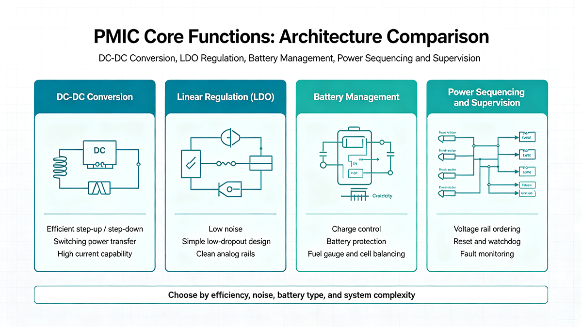
Modern PMICs typically integrate several key functions that work together to deliver reliable power to the entire system[reference:13]:
2.1. DC-DC Conversion
DC-DC converters form the backbone of PMIC power delivery. They step voltage up (boost) or down (buck) efficiently, maximizing battery life and minimizing heat generation[reference:14]. Buck converters are the most common type in PMICs-for instance, the TPS65219 from TI integrates three buck converters capable of supporting up to 3.5A for Buck1 and 2A each for Buck2 and Buck3[reference:15]. The switching frequency is typically in the range of 2.25 MHz to 3 MHz, enabling the use of small external inductors and capacitors[reference:16].
Some PMICs also include buck-boost converters that can step voltage up or down as needed. The TPS65216, for example, includes one adjustable buck-boost converter with integrated switching FETs, supporting output currents up to 1.6A[reference:17]. For applications requiring high-voltage outputs, Qorvo's ACT81461 includes a high-voltage step-up boost regulator capable of providing up to 20V[reference:18].
2.2. Linear Regulation (LDO)
Low-Dropout Regulators (LDOs) provide low-noise linear voltage regulation, which is critical for analog circuits, RF sections, and precision ADCs[reference:19]. LDOs operate by dissipating excess voltage as heat-they are simple, inexpensive, and produce very clean output with minimal noise[reference:20].
Most PMICs include multiple LDOs to power noise-sensitive loads. The TPS65219 integrates four LDOs, with LDO1 and LDO2 capable of 400mA each and configurable as load switches or bypass mode to support dynamic SD card voltages[reference:21]. The nPM1300 from Nordic Semiconductor includes two LDOs / load switches with output currents of 50mA (LDO mode) and 100mA (load switch mode), with output voltages programmable from 1.0V to 3.3V in 100mV steps[reference:22].
2.3. Battery Management
For battery-powered applications, PMICs often integrate comprehensive battery management functions including charging, fuel gauging, and protection[reference:23]. The TPS65070x series from TI includes a linear charger with up to 1.5A maximum charge current, power path management with 2A output current, and USB input current limiting options (100mA, 500mA, 800mA, 1300mA)[reference:24].
The nPM1300 takes battery management further with an algorithm-based fuel gauge that provides state of charge (SoC) and state of health (SoH) reporting[reference:25]. It supports Li-ion, Li-poly, and LiFePO₄ battery types with charge current programmable from 32mA to 800mA and termination voltage from 3.5V to 4.45V in 50mV steps[reference:26].
2.4. Power Sequencing and Supervision
Power sequencing controls the startup and shutdown order of voltage rails, preventing latch-up conditions and ensuring reliable boot-up[reference:27]. Many PMICs include programmable power sequencing-the TPS65219, for example, offers programmable power sequencing and default voltages, with integrated voltage supervisors for undervoltage protection on each rail[reference:28].
The nPM1300 provides comprehensive system management features including a hardware watchdog, power loss warning, hard reset supervisory circuit, failed boot recovery, ship mode (370 nA), and hibernate mode (500 nA)[reference:29][reference:30]. These features are essential for battery-powered IoT devices that require extended standby times and reliable system recovery.
3. Types of PMICs
Understanding PMIC categories helps narrow down selection quickly. Each type serves different applications and comes with distinct trade-offs[reference:31]:
| PMIC Type | Key Characteristics | Typical Applications | Example Devices |
|---|---|---|---|
| Multi-Channel PMICs | Multiple regulators, sequencing logic, supervisory functions in one package[reference:32] | SoCs, FPGAs, application processors with multiple voltage rails | TI TPS65216, TPS65219[reference:33][reference:34] |
| Battery Management PMICs | Charger, fuel gauge, power path, protection[reference:35] | Smartphones, wearables, portable devices | Nordic nPM1300[reference:36], TI TPS65070x[reference:37] |
| Low-Power PMICs | Ultra-low quiescent current, small package, optimized for battery life[reference:38] | IoT sensors, wearables, medical devices | Qorvo ACT81461[reference:39], TI TPS65720[reference:40] |
| High-Voltage PMICs | Wide input voltage range, integrated power loss protection | Enterprise SSDs, industrial, automotive | Qorvo ACT85611 (2.7V–14V input, 20V blocking)[reference:41] |
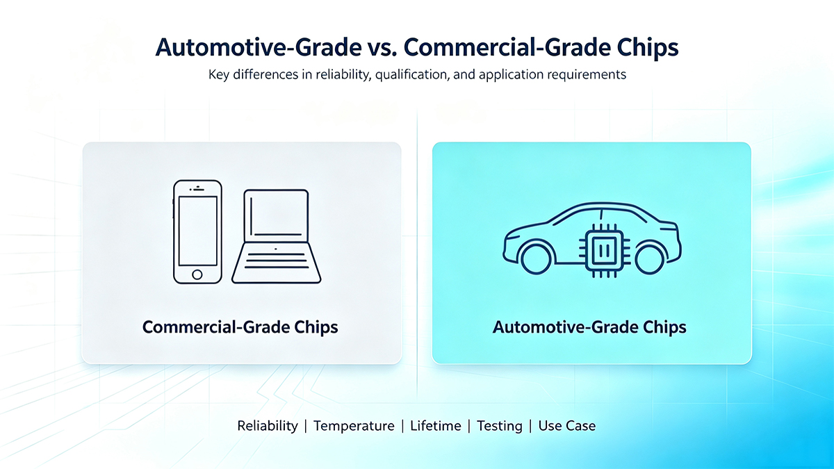
| Automotive PMICs | AEC-Q100 qualified, extended temperature range (-40°C to +125°C)[reference:42] | ADAS, infotainment, body electronics | TI TPS65219-Q1[reference:43], TPS65224-Q1[reference:44] |
4. Key Electrical Parameters for Selection
Selecting the right PMIC requires careful evaluation of several critical parameters. The following table summarizes the key specifications to consider, with example values from leading manufacturers:
| Parameter | Description | Typical Range | Example Device |
|---|---|---|---|
| Input Voltage Range (VIN) | Operating input voltage range the PMIC can accept |
2.7V – 5.5V (battery-powered)[reference:45] 5.6V – 21V (high-voltage)[reference:46] |
TPS65216: 2.7V–5.5V[reference:47] TPS650860: 5.6V–21V[reference:48] |
| Output Current per Rail | Maximum current each regulator can deliver |
200mA – 3.5A per buck[reference:49] 50mA – 400mA per LDO[reference:50][reference:51] |
TPS65219 Buck1: 3.5A[reference:52] nPM1300 LDO: 50mA[reference:53] |
| Quiescent Current (IQ) | Current consumed by PMIC in standby/no-load condition |
19 µA per converter (typ)[reference:54] 370 nA (ship mode)[reference:55] |
TPS65070x: 19 µA[reference:56] nPM1300: 370 nA ship mode[reference:57] |
| Switching Frequency | Operating frequency of DC-DC converters | 2.25 MHz – 3 MHz[reference:58][reference:59] |
TPS65070x: 2.25 MHz[reference:60] DA9066: 3 MHz[reference:61] |
| Output Voltage Accuracy | Regulation accuracy of output rails |
±1.5% (PWM mode)[reference:62] ±4% to ±5%[reference:63] |
TPS65070x: ±1.5%[reference:64] TPS65216: ±4%–±5%[reference:65] |
| Package Type | Physical package and footprint | QFN, WLCSP, BGA |
ACT81461: 3.3×3.3mm WLCSP[reference:66] TPS65216: 48-QFN[reference:67] |
| Interface | Digital control interface for configuration and monitoring | I²C, SPI |
TPS65216: I²C (400kHz)[reference:68] nPM1300: I²C-compatible TWI[reference:69] |
For battery-powered devices, quiescent current (IQ) is particularly critical because it determines standby battery life[reference:70]. The nPM1300 achieves ship mode consumption as low as 370 nA and hibernate mode at 500 nA[reference:71], making it suitable for wearable and IoT applications that spend most of their time in standby.
Efficiency is another crucial parameter-especially light-load efficiency, since many systems operate in low-power states for extended periods[reference:72]. The nPM1300 achieves power conversion efficiency up to 93%[reference:73], while the DA9066 from Renesas specifies efficiency of 85% at 300mA load[reference:74].
5. PMIC Design and PCB Layout Guidelines
Proper PCB layout is essential for achieving optimal performance from a PMIC. Switching regulators require careful layout to minimize noise and maximize efficiency[reference:75]. Even a well-selected PMIC will perform poorly if layout practices introduce excessive parasitics or thermal issues.
5.1. Thermal Management
The exposed pad (EP) is the main path for heat to exit the IC. Connect the EP to the ground plane with thermal vias to allow heat to dissipate from the device[reference:76]. The top layer ground area should be connected to internal ground layers using vias at the input bypass capacitor, the output filter capacitor, and directly under the PMIC device to provide a thermal path[reference:77].
For good thermal coupling, a 4-layer PCB layout is recommended, with PCB vias required from the exposed pad to the ground plane[reference:78]. Multiple ground planes-for example, a mid-layer and bottom layer plane-are helpful to control high-frequency noise and improve thermal resistance[reference:79].
5.2. Routing and Component Placement
Layout is a critical portion of PMIC designs[reference:80]. Key guidelines include:
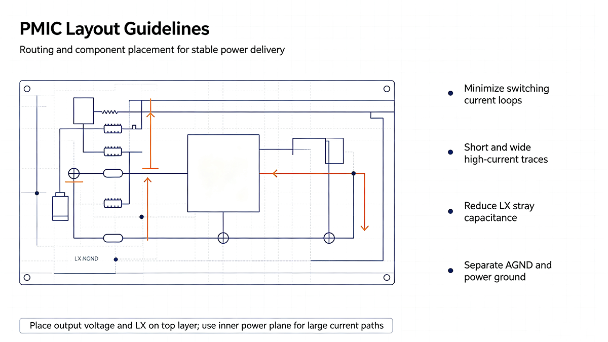
- Minimize switching current loops: Place the input capacitor, inductor, and output capacitor with tight component placement and minimal return path to the PMIC thermal pad[reference:81].
- Short and wide traces: Use short and wide traces for high-current paths to minimize parasitic resistance and inductance[reference:82].
- Avoid stray capacitance: Minimize stray capacitance on switching nodes (LX) to maintain high efficiency and reduce EMI[reference:83].
- Separate analog and power grounds: Connect the dedicated AGND pin of the PMIC to an internal layer via, rather than directly to the noisier thermal pad on the top layer[reference:84].
- Place tracing for output voltage and LX on the top layer, with an inner power plane for VIN[reference:85].
5.3. Capacitor Selection and Derating
The voltage rating of selected capacitors should consider derating-a commonly used guideline is to select capacitors with a voltage rating greater than twice the worst-case applied voltage[reference:86]. For example, the TPS6521505-Q1 buck converters require a small 470 nH inductor and 4.7 µF input capacitance[reference:87]. Always consult the PMIC datasheet for specific component recommendations.
6. Common Failures and Troubleshooting
Understanding common PMIC failure modes helps engineers design more reliable systems and debug issues efficiently[reference:88]:
- Electrical Overstress (EOS): The most common "fatal killer" of PMICs. Input voltage transients exceeding the absolute maximum rating can destroy internal FETs. Always verify the maximum input voltage (VIN_MAX) and transient withstand capability[reference:89].
- Latch-up: A "hidden killer" that can occur when parasitic SCR structures are triggered by voltage or current spikes. Proper power sequencing and input protection help prevent latch-up conditions[reference:90].
- Thermal Stress: Slow "aging catalyst" caused by inadequate heat dissipation. QFN packages require proper thermal pad connection to the ground plane[reference:91].
- Power-up failures: Common symptoms include the PMIC failing to power up, powering up but then shutting down unexpectedly, or failing to restart after power-off[reference:92]. These issues often trace back to incorrect sequencing, soldering faults, or inadequate decoupling[reference:93].
- ESD Damage: Electrostatic discharge during handling or assembly can damage sensitive PMIC inputs. Use appropriate ESD protection measures[reference:94].
- Overload and Short Circuits: Excessive load current or output short circuits can trigger thermal shutdown or cause permanent damage. Ensure the PMIC's overcurrent protection is appropriately configured[reference:95].
7. Reliability Verification and Testing
To guarantee long-term reliability, the following tests should be performed during design validation:
- Input voltage transient test: Verify PMIC behavior under input voltage steps and transients to ensure it remains within specification.
- Load transient response test: Apply load steps and measure output voltage deviation and recovery time to verify regulation performance.
- Thermal imaging and temperature cycling: Verify that all components remain within their rated temperature ranges under worst-case operating conditions.
- Power sequencing validation: Use an oscilloscope to measure the startup and shutdown sequence of all rails to confirm compliance with processor or FPGA requirements.
- EMI/EMC testing: Verify that the PMIC design meets applicable electromagnetic compatibility standards, particularly for automotive and industrial applications.
8. PMIC Design Checklist
- Define all required voltage rails, including voltage, current, and noise requirements for each load[reference:96].
- Determine input voltage range and transient withstand capability-for battery-powered devices, typical VIN is 2.7V–5.5V[reference:97].
- Calculate total power dissipation and verify thermal derating-operate PMIC well below its maximum junction temperature.
- Select a PMIC with sufficient output current per rail-for example, TPS65219 provides 3.5A on Buck1[reference:98].
- Verify quiescent current (IQ) meets standby power targets-critical for battery-powered applications[reference:99].
- Confirm power sequencing requirements-programmable sequencing is available on devices like TPS65216 and TPS65219[reference:100][reference:101].
- Select appropriate external components (inductors, capacitors) per datasheet recommendations[reference:102].
- Follow PCB layout guidelines: thermal vias under exposed pad, short switching current loops, separate analog and power grounds[reference:103][reference:104].
- Implement input protection (TVS, overvoltage protection) for harsh environments[reference:105].
- Verify I²C/SPI communication and register configuration for programmable PMICs[reference:106].
- Perform thorough testing under worst-case conditions: temperature extremes, load transients, and input voltage variations.
9. Frequently Asked Questions (FAQ)
A PMIC integrates multiple power management functions-such as DC-DC converters, LDOs, battery chargers, and power sequencing-into a single chip, whereas a discrete design uses separate components for each function[reference:107]. PMICs reduce board space, BOM cost, and design complexity, while discrete designs offer greater flexibility for high-current or specialized applications.
Key selection criteria include: input voltage range (e.g., 2.7V–5.5V for battery-powered devices[reference:108]), number and type of output rails (buck converters, LDOs), output current capability per rail, quiescent current for standby efficiency[reference:109], switching frequency, package size, and interface (I²C/SPI). Always consult the manufacturer's datasheet for derating curves and thermal considerations.
Power sequencing controls the order in which different voltage rails are powered up and shut down during system startup and shutdown[reference:110]. Proper sequencing prevents latch-up conditions, ensures reliable boot-up of processors and FPGAs, and protects downstream components from incorrect voltage application. Many PMICs, such as the TI TPS65216, include integrated programmable power sequencing[reference:111].
Quiescent current (IQ) is the current consumed by the PMIC itself when the load is inactive or in standby mode[reference:112]. Low IQ is critical for battery-powered devices to maximize standby time. For example, the TI TPS65070x series specifies a typical quiescent current of 19 µA per converter[reference:113], while Nordic's nPM1300 achieves ship mode consumption as low as 370 nA[reference:114].
Common failure modes include electrical overstress (EOS) from input voltage transients exceeding the absolute maximum rating[reference:115], thermal stress from inadequate PCB heat dissipation[reference:116], latch-up conditions from improper power sequencing[reference:117], ESD damage during handling[reference:118], and solder joint faults causing intermittent connections[reference:119]. Proper derating, thermal management, and layout practices are essential for reliability.
10. Industry Trends and Outlook
The PMIC market continues to evolve rapidly, driven by demands for higher efficiency, smaller form factors, and greater integration. Key trends shaping the industry include:
- Ultra-low quiescent current: Wearable and IoT applications are pushing PMIC standby currents into the nanoampere range-the nPM1300 achieves 370 nA in ship mode[reference:120].
- Increased integration: PMICs are incorporating more functions-fuel gauges, ADC monitoring, watchdog timers, and LED drivers-reducing external component count[reference:121].
- Automotive-grade PMICs: AEC-Q100 qualified devices with extended temperature ranges (-40°C to +125°C) are increasingly in demand for ADAS, infotainment, and electrification applications[reference:122].
- Digital control and programmability: I²C/SPI interfaces with real-time configurability are becoming standard, enabling dynamic voltage scaling and adaptive power management[reference:123].
- High-voltage and power-loss protection: PMICs with integrated power loss protection (PLP) are emerging for enterprise storage and industrial applications-the ACT85611 from Qorvo combines PLP with PMIC functions in a single chip[reference:124].
- Miniaturization: Packages as small as 3.3×3.3 mm WLCSP enable PMICs in space-constrained wearables and medical devices[reference:125].
11. Conclusion
Power Management Integrated Circuits (PMICs) are essential components in modern electronic systems, providing the centralized power management needed for complex SoCs, FPGAs, and battery-powered devices[reference:126]. By consolidating multiple power management functions-DC-DC converters, LDOs, battery chargers, power sequencing, and supervisory circuits-PMICs reduce board space, simplify design, and improve system reliability.
Successful PMIC design requires careful attention to key parameters: input voltage range, output current capability, quiescent current, switching frequency, and thermal management. Proper PCB layout-including thermal vias under the exposed pad, short switching current loops, and separate analog and power grounds-is essential for achieving optimal performance[reference:127][reference:128]. By following best practices in selection, layout, and testing, engineers can create robust power delivery systems that meet the demanding requirements of today's electronic devices.